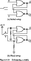
Figure 6.56(a) shows the initial setup, a single
pole/double throw (SPDT) switch and an R-S
latch. We should get a 0 at the output Q when we place the switch
in one position and a 1 at Q when we place it in the opposite position.
Since the holding state occurs when R and S are both 0,
we want these to be the default values while the switch is in transition
between its settings. The switch must be able to force one of these inputs
to a 1 depending on its current setting.
This setup leads to the wiring diagram of Figure 6.56(b).
The single contact side of the switch is connected to the power supply while
the double contact side is connected to the R and S inputs
of the latch. When the switch is connected to the top output, R
is asserted and Q is reset to 0. When it is placed in the lower
position, S is asserted and Q is set to 1.
This diagram does not yet solve the bounce problem. We
must ensure that when the switch is not connected to one side, the latch
input remains steady at 0. To accomplish this, we wire both R and
S to ground through resistors. The resistors are sized so that
the input can be pulled high when the switch is trying to do so. They also
protect the circuit against a short circuit between ground and the power
supply.
When the switch is in the reset position, the R
input to the latch is set high and Q is low. Now suppose that the
switch is in transition from the R to the S position.
The switch breaks connection with the R terminal, and the ground
connection pulls the latch input low. The latch is now in its holding state
because both inputs are 0.
When the switch first touches the S contact,
the S input to the latch goes high, and the latch is set with Q
equal to 1. If the switch bounces, temporarily breaking the connection,
the latch input returns to 0, leaving the latch in the holding state. If
the switch bounces back, remaking the S connection, the latch is
simply set again and no state change occurs.
As long as the switch does not bounce far enough to remake
the R connection, the Q output will remain high as long
as the switch is bouncing into its final setting position. The same analysis
applies for a switch transition from resting at the S terminal
to connecting the R -terminal.
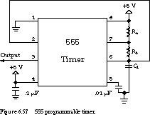
The period and duty cycle are controlled by placing the appropriate resistors
and capacitors between the 555 timer's pins, as shown in the figure.
The following formulas describe the relationships between the resistors,
the capacitor, and the generated clock's characteristics:
= 0.7(Ra
+ Rb)C1= 0.7(Rb)C1= high time + low time =
0.7(Ra + 2Rb)C1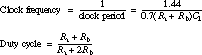
Example Capacitance is measured in farads, resistance
is in ohms, and R C = farads ohms =
seconds (you may want to review Appendix B if this is foreign
to you). Suppose we want to design a clock signal with a period
of approximately 500 µs and a 75% duty cycle. This is a frequency of
2000 hertz, written as 2 kHz. The first step is to
determine the ratio of the resistors needed to obtain the desired duty cycle.
Substituting into the duty cycle formula, we obtain
The duty cycle is completely determined by the ratio
of the resistors, not their specific values.
To achieve the 75% duty cycle, Ra should have
twice the resistance of Rb. Suppose that we choose Ra
= 5000 Rb = 2500 C1:
In terms of practical design, it may not be possible
to obtain exactly the desired clock signal with the resistors and capacitors
at hand. Suppose we have only 0.1-µF capacitors. Substituting one of
these in the equations yields a clock with period 700 µs and a high
time of 525 µs. This is somewhat slower than our design goal.
Alternatively, we could replace Ra with a 3600-Rb
with an 1800-C1 a 0.1-µF capacitor, we obtain a clock with
period 504 µs and a 75% duty cycle. This is quite close to our desired
clock waveform.

Figure 6.58 gives a chart that plots the free-running timer frequency
as a function of Ra + 2Rb and C1.
This chart is useful for identifying approximate values for the resistors
and capacitors to obtain a clock of a particular frequency. For example,
it is easy to see that a 0.1-µF capacitor and resistors such that Ra
+ 2Rb = 7200
A Practical Warning The 555 timer
draws large amounts of current for short periods of time when the output
changes state. For this reason, it is important to put a 0.1-µF bypass
capacitor from the 5-V pin, pin 4, on the 555 to ground. This capacitor
will minimize spikes that can upset the rest of your circuit. In general,
it is good practice to put bypass capacitors liberally throughout your design
on the power pins of ICs.
[Top] [Next]
[Prev]