
1. (Simple Circuits with Feedback) Build
a feedback circuit with cross-coupled NAND gates. What input conditions
cause the state of this latch-like device to be reset? To be set? Does this
circuit have forbidden inputs? If so, what are they? 2. (Simple Circuits with Feedback) An
R-S latch can be used to determine which of two events
has occurred first. Design a circuit with three inputs and three outputs
that determines which of three single pole/single throw switches connected
to the inputs has been opened first. The circuit will produce a logic
1 on the output that corresponds to that input. Discuss how you would expand
this circuit to a larger number of inputs, say 12 inputs or 30 inputs. 3. (Setup and Hold Times) Imagine
that it is possible to have storage devices with negative setup and hold
times. What do you think such a concept would be? Draw timing diagrams to
illustrate your answer. 4. (D Flip-Flop) Add preset and
clear inputs to the edge-triggered D flip-flop of Figure
6.24. Draw the logic schematic of the revised -circuit. 5. (D Flip-Flop) How would you implement
a negative edge-triggered D flip-flop using NAND gates only?
What changes are necessary to make this a positive edge-triggered device?
6. (J-K Flip-Flop) How would you
implement a J-K master/slave flip-flop, such as
the circuit in Figure 6.22, using NAND gates only? Assume the master and
slave latches are actually controlled by the signals 7. (J-K Flip-Flop) Starting with
the basic circuit schematic for the -master/slave J-K
flip-flop, show how to add asynchronous preset and clear inputs to
force the flip-flop into a 1 (preset) or
0 (clear) state. Draw a timing waveform for the
preset input, clear input, clock, -master stage outputs (P,
), and slave stage outputs (Q,
) showing the operation of preset and clear.
8. (J-K Flip-Flop) J-K
master/slave flip-flops exhibit the phenomenon of ones catching. Briefly explain why this takes place. Can a master/slave flip-flop catch
0's? Explain why or why not. 9. (Flip-Flops) The basic functionality
of a D flip-flop can be implemented by a J-K
flip-flop simply by connecting the input signal D to the
J-K flip-flop's J input and Draw a timing waveform for the clock, input D, and outputs Qpos, Qneg, and Qms that illustrates the differences in input/output behavior of a positive edge-triggered D flip-flop, negative edge-triggered D flip-flop, and master/slave D flip-flop(implemented from a J-K master/slave flip-flop as described in Figure 6.22). Include some transitions on D while the clock is asserted.
10. (Flip-Flops) Given the input
and clock transitions given in Figure Ex6.13, draw a waveform for the output
of a J-K device, assuming: It is a
master/slave flip-flop. It is a positive edge-triggered flip-flop.
It is a negative edge-triggered flip-flop. You may assume 0 setup, hold, and propagation times, and that the initial state of the flip-flop is 0.
11. (Flip-Flops) Given the input
and clock transitions in Figure Ex6.11, indicate the output of a D
device assuming: It is a negative edge-triggered flip-flop.
It is a master/slave flip-flop.
It is a positive edge-triggered flip-flop.
It is a clocked latch. You may assume 0 setup, hold, and propagation times.

12. (Flip-Flops) Identify the
following statements as either true or false:
The inputs to a level-sensitive latch always affect its outputs.
Flip-flop delays from the change in the clock edge to the change in the output are typically shorter than flip-flop hold times, so shift registers can be constructed from cascaded -
flip-flops.
Assuming zero setup and hold times, clocked latches and flip-flops produce the same outputs as long as the inputs do not change while the clock is asserted.
A master/slave flip-flop behaves similarly to a clocked latch, except that its output can change only near the rising edge of the clock.
An edge-triggered D flip-flop requires more internal gates than a similar device constructed from a J-K master/slave flip-flop.
13. (Flip-Flops) Match each of the
following five circuits (Figure Ex6.13) with
the phrase that best describes it from the list:
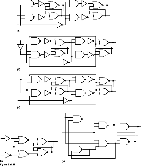
(1) clocked R-S latch, (2)
clocked D latch, (3) master/slave R-S
flip-flop, (4) positive edge-triggered R-S
flip-flop, (5) negative edge-triggered R-S
flip-flop, (6) master/slave D flip-flop, (7) positive edge-triggered D
flip-flop, (8) negative edge-triggered D
flip-flop, (9) master/slave T flip-flop, (10) positive edge-triggered T
flip-flop, (11) negative edge-triggered
T flip-flop, (12) master/slave
J-K flip-flop, (13) positive
edge-triggered J-K flip-flop, (14)
negative edge-triggered J-K flip-flop.
14. (Flip-Flops) Any flip-flop type can be implemented from another type with suitable logic applied
to the latter's inputs. Show how to implement a J-K flip-flop starting with a D flip-flop.
15. (Flip-Flops) Show how to implement
a J-K flip-flop starting with a T flip-flop.
16. (Flip-Flops) Show how to implement
a D flip-flop starting with a J-K flip-flop.
17. (Flip-Flops) Show how to implement
a D flip-flop starting with a T flip-flop.
18. (Flip-Flops) Show how to implement
a T flip-flop starting with a J-K flip-flop.
19. (Flip-Flops) Show how to implement
a T flip-flop starting with a D flip-flop.
20. (Clock Generator) Extend the
circuit of Figure 6.37 to generate a three-phase nonoverlapping clock. How
would the circuit be extended to generate a four-phase nonoverlapping clock?
21. (Clock Skew) Given the timing
specification of the 74LS74 flip-flop of Figure 6.14, what is the
worst-case skew in the clock that could be tolerated when one 74LS74 needs
to pass its value to another 74LS74, as in Figure 6.29?
22. (Clocking Issues) Given the
sequential logic circuit of Figure Ex6.22, where the flip-flops have
worst-case setup times of 20 ns, propagation delays of 13 ns, and hold times
of 5 ns, answer the following questions:
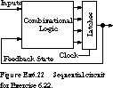
Assuming 0 propagation delay through the combinational logic block, what is the maximum allowable frequency of the clock that controls this subsystem?
Assuming a typical combinational logic delay of 75 ns and a worst-case delay of 100 ns, how does your answer to part(a)change?
23. (Two-Phase Clocking) Consider
the two-phased clocked sequential circuit of Figure Ex6.23. Assume that
the f1 and f2 latches have 5-ns setup times, 5-ns
hold times, and 10-ns propagation delays in the worst case. Given that the
combinational logic block has a maximum delay of 100 ns and a typical delay
of 75 ns, what is the shortest possible period between the rising edge of
f1 and the falling edge of f2? Show how you obtained
your result.

24. (Metastability) You have designed a high-performance
disk drive interface. The interface has an internal clock rate of 25 MHz,
and asynchronous commands from a computer with a different clock are presented
every 200 ns. It works fine, but every few days or weeks it has random
operational failures that cause loss of data. There are no component failures,
software bugs, or power glitches, and the errors occur mainly for customers
who use the interface heavily. Suggest a possible cause of these failures
and how you could change the design to reduce the failure rate.
25. (Metastability) One way to reduce the probability
of synchronizer failure is to place two synchronizer flip-flops in
series between the asynchronous input and the rest of the synchronous digital
system. Why do you think this reduces the problem of metastability?
26. (Delay Insensitive Handshaking) Draw a simple
flowchart for the master side and the slave side algorithms of the four-cycle
handshake. Repeat for the two-cycle handshake. How does the complexity of
the two approaches compare?
27. (Practical Matters) How would the debounce
circuit of Figure 6.56 change if you were to use an ![]() -
-![]() latch instead of
an R-S latch?
latch instead of
an R-S latch?
28. (Practical Matters) Suppose you are to design
a debouncing circuit using a single pole/single throw (SPST)
switch. Can it be done? What problems do you face?
29. (Practical Matters) Given the discussion
of the 555 timer chip, is it possible to obtain duty cycles of less than
50%? If it is, give an example of resistor ratios needed to obtain such
a duty cycle. If not, explain why and give a possible scheme for deriving
a waveform with less than a 50% duty cycle from the 555's output.
30. (Practical Matters) Use the equations given
in Section 6.6.2 and the chart in Figure 6.58 to configure the 555 timer
according to the following specifications. Show all of your intermediate
work, coming as close to the specification as you can:
Choose resistors and a capacitor to obtain a 100-kHz clock with 67% duty cycle.[Top] [Next] [Prev]
Choose resistors to obtain a 1 MHz clock with 75% duty cycle using a 0.1-µF capacitor.
Choose resistors and a capacitor to obtain a clock period of 140 µs and 75% duty cycle.
Given a clock period of 1 µs, Ra=9 kRb=1 k.