(and frequently is)
the 60-cycles-per-second alternating current that is delivered to your house
by the power company. A sequential circuit counts the number of transitions
in the reference signal to determine when to perform some action, such as
advancing the clock. Interestingly, this independent signal oscillating
at a known frequency is often called a clock. (north-south green/east-west
red, north-south yellow/east-west red, north-south red/east-west green,
north-south red/east-west yellow), stored in special circuit
structures called memory elements. Although the traffic light controller
is a sequential circuit in its own right, these memory elements are the
simplest, most primitive sequential circuits. (random-access
memory) designs. Alternatively, we can build a simple memory
structure from cross-coupled NOR and NAND gates. These two types of memory
elements form the basic building blocks of the latch and flip-flop memory
elements we will introduce in this chapter. We begin our examination of
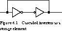
sequential logic with these very primitive structures. Inverter Chains Consider the almost trivial circuit
of Figure 6.1. It contains nothing more than two inverters in series, with
the output of the second-stage inverter fed back as input to the first-stage
inverter. A logic 1 at the input of the first inverter becomes a 0 at
its output. The 0 is mapped to a logic 1 at the output of the second stage,
which reinforces the value at the first inverter's input. A similar argument
holds for a 0 at the input. Once a value is inserted at the input, it can
be held indefi-nitely by the circuit.
Of course, the problem with this circuit is how to get
a value into the memory element in the first place. Some value will be
there when power starts up, but for this circuit to be an effective building
block, we must be able to select the value to be stored. We need extra logic
to set the memory element to a specific value. The feedback path must
be broken while a new value is connected to the input.
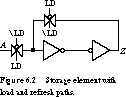
One way to build such a memory element is shown in Figure 6.2, where
CMOS transmission gates are used to implement a 2:1 multiplexer on the inputs
to the memory element. When we assert LD (load),
the feedback path is broken, and the value at input A can be stored
in the element. When LD is unasserted, the input from A is broken,
and the feedback path is reestablished. Note that because of the critical
nature of the timing of the signals in these kinds of circuits, many logic
simulators have difficulty in modeling such signal flows, even though the
physical circuit would operate without difficulty.
Cascaded inverters can serve a purpose besides storage.
They can be used to build circuits whose outputs oscillate between low and
high voltages. Such circuits are called ring oscillators.
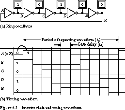
Figure 6.3(a) shows an inverter chain, and
Figure 6.3(b) gives the associated timing waveform.
The timing waveform begins with node A (also labeled
X) about to switch from 0 to 1.
The odd number of inverters leads to oscillatory behavior
that repeats every tp time units. This is called the period
of the signal. Duty cycle is defined as the percentage of time
a signal is high during its period. In the figure, the signal has a 50%
duty cycle.
In the ring oscillator, the duration of the period depends
on the number of inverters in the chain. In this case, we have five inverters
with unit delay (that is, a gate delay of 1 time unit).
The high time of the waveform is five time units: five times the gate
delay of a single stage. If we had a seven-inverter chain, the period would
be 14 time units: seven units high, seven units low.
To see why this is the case, let's examine Figure 6.4.
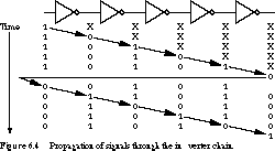
Each row gives the logic state associated with the nodes of the circuit.
The rows differ in time by a single gate delay. Starting with a 1 at the
input to the first stage, the signal propagates through the inverters,
alternating its logic value between the stages. Once the signal emerges
from the last stage, it is fed back to the first stage as the complemented
value. The propagation repeats. In examining any node in the circuit, we
discover that it stays high or low for exactly five gate delays.
Cross-Coupled NOR Gates as a Basic Memory Element An
alternative method for building circuits with state is to use cross-coupled
NOR gates (NAND gates can be used in a similar fashion).
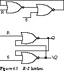
Figure 6.5 shows two alternative ways to represent cross-coupled NORs.
Recall that a NOR gate with a 0 input acts like an inverter with respect
to the other input: if the nonzero input is 1, the NOR's output is 0, and
if it is 0, the NOR's output is 1. Similarly, if one of the NOR's inputs
is 1, the output is always 0. One of the NOR gates of Figure 6.5 acts like
an inverter while the other injects a 0, depending on the settings of the
R and S inputs.
Suppose R = 1 and S =
0. Since the R input is 1, the Q output is reset
to 0 independent of the ![]() input to the first NOR gate.
With S at 0, the Q input is inverted to form the
input to the first NOR gate.
With S at 0, the Q input is inverted to form the ![]() output. R is called the reset input.
output. R is called the reset input.
Now suppose that R = 0 and S
= 1. The same arguments apply as in the previous case. ![]() is reset to 0. When this output is fed back to the first NOR
gate, it is inverted, and Q is set high. Hence S
is called the set input. When R and S are both 0, the
NOR gates behave like chained inverters and will hold their current output
values indefinitely. This configuration of NOR gates is called an
R-S latch.
is reset to 0. When this output is fed back to the first NOR
gate, it is inverted, and Q is set high. Hence S
is called the set input. When R and S are both 0, the
NOR gates behave like chained inverters and will hold their current output
values indefinitely. This configuration of NOR gates is called an
R-S latch.
Timing Behavior of the Cross-Coupled NOR Gates The
timing behavior of these gates is shown in the timing waveform of Figure
6.6.
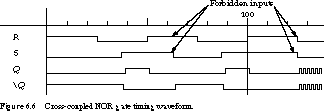
Q is set high when S is asserted and is reset low when
R is asserted. Whenever R and S are both zero,
the outputs remain unchanged.
What happens when both R and S are
asserted? Q cannot be both 1 and 0 simultaneously! This input condition
is forbidden in normal operating conditions. Both Q and
![]() are driven to 0, violating the assumption that the two
outputs are always complements of each other.
are driven to 0, violating the assumption that the two
outputs are always complements of each other.
When one of R or S is returned to the
unasserted state, the remaining asserted signal determines the steady-state
output values of Q and ![]() . In the first case
of forbidden inputs in Figure 6.6, R remains asserted while S
is left unasserted. Q stays at 0, while
. In the first case
of forbidden inputs in Figure 6.6, R remains asserted while S
is left unasserted. Q stays at 0, while ![]() goes to 1. Comparable
behavior will be observed if R becomes unasserted while S
stays asserted.
goes to 1. Comparable
behavior will be observed if R becomes unasserted while S
stays asserted.
Now suppose that R and S return to
0 simultaneously. This is the second case of forbidden inputs in Figure
6.6. The outputs actually oscillate. Q and ![]() are initially
0. When R and S go to 0, the NOR gate outputs go to 1.
But when these are fed back to the inputs, the NOR gates behave like inverters,
switching the outputs back to 0. This oscillatory behavior is called a race
condition.
are initially
0. When R and S go to 0, the NOR gate outputs go to 1.
But when these are fed back to the inputs, the NOR gates behave like inverters,
switching the outputs back to 0. This oscillatory behavior is called a race
condition.
Theoretically, the race condition can continue as long
as R and S are 0. However, the delay through the two NOR
gates is not perfectly matched, and one of Q and ![]() will be driven
to a new value before the other, stopping the oscillations. To avoid the
race condition, we restrict the R and S inputs never to
be 1 at the same time.
will be driven
to a new value before the other, stopping the oscillations. To avoid the
race condition, we restrict the R and S inputs never to
be 1 at the same time.
We summarize the behavior of the cross-coupled NOR gates
in the functional truth table of Figure 6.7.
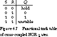
When R = S = 0, the circuit
holds its current output-in other words, the output is the same as it was
for the last setting of the inputs. When one of R or S
is set to 1, the output is forced to 0 or 1, respectively. When both inputs
are 1, the outputs oscillate between 0 and 1.
Another representation of the behavior of cross-coupled
gates is called the state diagram. The diagram consists of nodes
and arcs. The nodes represent unique configurations or states of the
circuit. The arcs are labeled with the input combinations that cause a transition
from one state to another.
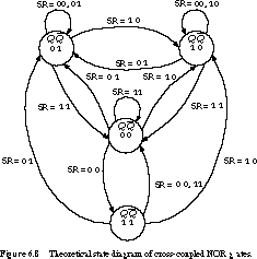
Figure 6.8 shows the state diagram for the cross-coupled NOR gates. The
circuit's state depends on the values of the outputs Q and ![]() , so there are four possible states, one for each combination of
possible values for the two outputs. Since there are two inputs, S
and R, there are exactly four transitions from each state, one
for each of the possible input combinations.
, so there are four possible states, one for each combination of
possible values for the two outputs. Since there are two inputs, S
and R, there are exactly four transitions from each state, one
for each of the possible input combinations.
The states labeled 01 and 10 are the normal configurations
of the circuit. When set (S) is asserted,
we enter state 10 (Q = 1, ![]()
=
0). When reset (R) is asserted,
we change to state 01 (Q = 0, ![]()
= 1). When S and R
are both 0, we hold in the current state.
When we encounter the forbidden input configuration
S = R = 1, the circuit enters
state 00. It stays in this state as long as these inputs are asserted. As
soon as one input returns to 0, the circuit returns to state 01 or 10.
If the current state is 00 and S =
R = 0, the circuit enters state 11. It does not stay
there very long, immediately returning to state 00 if S and R
remain 0. If the delays through the gates are perfectly matched, the circuit
can oscillate between these two states forever. Of course, this does not
make a very useful memory element.
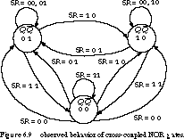
Figure 6.9 gives a state diagram we constructed by observing the behavior
of a real cross-coupled NOR gate circuit. The actual circuit does not oscillate
between 00 and 11 indefinitely, but rather ends up sometimes in state 10
and sometimes in state 01. This is the true meaning of a race condition
in sequential logic: the resulting state depends on the circuit's time-dependent
behavior and cannot be predicted in advance. The race condition is most
easily avoided by never putting the circuit into state 00 in the first place.
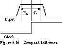
These concepts are shown in Figure 6.10 for a rising clock edge event.
The input must remain stable at least a setup time before the reference
clock edge and at least a hold time after the edge for the input signal
to be recognized as a logic 1. If these constraints are not satisfied,
the input may be interpreted as a 1 or a 0 or some unrecognizable value
between 0 and 1. It is extremely dangerous to allow input signals to change
very close to the sampling event, as we shall see in Section 6.4.
Latches and Flip-Flops Let's return
to the concept of the sampling event. Think of this event as an enable signal
that instructs the memory element to examine its input to change its state.
We can use a single clock to synchronize the update of many memory elements
in our system.
Figure 6.5 already showed the basic R-S
latch. Primitive memory elements actually fall into two broad classes: latches
and flip-flops. When the memory element's outputs immediately change
in response to input changes, they are called transparent outputs.
The R-S latch has transparent outputs.
If a latch has only data inputs, like R and
S, it is called an unclocked latch. Level-sensitive latches
have an additional enable input, sometimes called the clock.
Level-sensitive latches continuously sample their inputs
while they are enabled. Any change in the level of the input is propagated
through to the output.
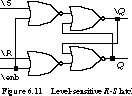
The circuit shown in Figure 6.11 is a level-sensitive latch. The holding
state occurs when both inputs are 1, the forbidden state when both inputs
are logic 0, the latch is set when ![]()
= 0, ![]()
= 1, and the latch is reset when ![]()
=
1, ![]()
= 0. The enable signal is also active low.
When it is high, the output from the first stage of NOR gates is forced
to 0, thus placing the cross-coupled second stage in the holding state.
When the enable signal is unasserted, the last value
of the inputs determines the state held by the latch. The "latched"
value is determined by the window formed from the setup and hold times around
the falling (high-to-low) edge of the enable signal.
Flip-flops differ from latches in that their outputs
change only with respect to the clock, whereas latches change output when
their inputs change. We can characterize flip-flops on the basis of the
clock transition that causes the output change: there are positive edge-triggered,
negative edge-triggered, and master/slave flip-flops.
A positive edge-triggered flip-flop samples its inputs
on the low-to-high clock transition. To be properly recognized, the input
must be stable within the setup and hold time window around the clock edge.
The outputs change a propagation delay after the rising clock transition.
A negative edge-triggered device works in a similar fashion,
with the input sampled on the high-to-low clock transition. The outputs
change a propagation delay after the falling edge of the clock. Under this
classification, a master/slave flip-flop is indistinguishable from the
negative edge-triggered device, except that it exhibits a strange behavior
called "ones catching," which we will discuss later.  Table 6.1 summarizes the different attributes of latches
and flip-flops.
Table 6.1 summarizes the different attributes of latches
and flip-flops.
Timing Examples To better understand
the terms just introduced, let's consider two memory elements: a positive
edge-triggered flip-flop (such as a TTL 74LS74)
and a level-sensitive latch (such as a 74LS76).
Each has a single data input D, a clock input C, and an
output Q. The block diagrams are shown in Figure 6.12.
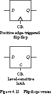
We normally represent edge-triggered devices with the clock input as
a triangle. A negative edge-triggered device has an additional negative
logic bubble at the clock input.
We compare the timing behavior of the two types of devices
in Figure 6.13.
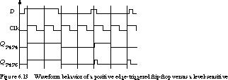
The outputs differ only when the input changes while the clock is asserted.
This is because the latch immediately responds to changes in the input while
the clock is high but the flip-flop does not.
The definitions of the setup and hold times are quite
different for these two devices.
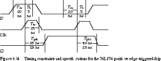
Figure 6.14 gives the timing waveforms for the 74LS74 positive edge-triggered
flip-flop. Tsu is 20 ns and Th is 5 ns. In addition, the
clock signal has a minimum duration, Tw = 25 ns. The
figure also defines Tphl, the propagation delay between the
rising edge of the clock and the change in the output from high to low,
and Tplh, the propagation delay from the rising clock edge to a
low to high change in the output. Tphl is 40 ns maximum, 25 ns
typical, and Tplh is 25 ns maximum, 13 ns typical.

Figure 6.15 displays the timing specifications for the 74LS76 clocked
transparent latch. As for the flip-flop, the quantities Tsu, Th,
and Tw are defined to be 20 ns, 5 ns, and 20 ns, respectively.
However, the setup and hold times are defined relative to the falling
edge. The specifications for Tphl and Tplh are more complex,
because they must be defined for two different events: from when the
input changes to a corresponding change in the output (D
» Q) and from when the clock becomes asserted
to when the output changes (C » Q).
Of course, the clock must be asserted before the input can influence
the output. Tphl (D » Q)
is 16 ns maximum, 7 ns typical; Tphl (C »
Q) is 25 ns maximum, 14 ns typical; Tplh
(D » Q) is 27 ns maximum,
15 ns typical; and Tplh (C » Q)
is 27 ns maximum, 15 ns typical.
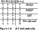
Note that the inputs are S, R, and Q at a
given time t, and the output is Q at time t +
ý, where ý represents a small increment in time. Q(t)
is the current state of the latch, and Q(t
+ ý) is the next state.
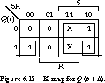
A K-map for the truth table is given in Figure 6.17. We can
derive the following so-called characteristic equation to describe the next
state in terms of the inputs and current state:
This equation is a convenient shorthand for describing
the memory element's behavior. For example, if S =
1 and R = 0, the next state Q+
becomes 1 independent of the current state. When S =
0 and R = 1, the next state is forced to be 0, independent
of the current state.
Level-Sensitive R-S
Latch The gated R-S latch is an extension
of the basic R-S latch that we saw in Figure 6.11. This
device adds the ability to latch a new state under the control of an external
enable signal. When the enable signal is asserted, the circuit's R
and S inputs affect the state. When enable is not asserted, the
latch holds its current state.
The timing behavior of the level-sensitive R-S
latch is shown in Figure 6.18.
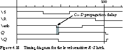
The propagation delay from when the clock is asserted to when the output
changes (C » D) is shown
in the diagram.
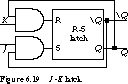
By feeding the Q and ![]() outputs back to the
inputs and gating these with external set and reset control inputs
outputs back to the
inputs and gating these with external set and reset control inputs (now
called J and K, respectively), we guarantee
that the internal R and S are never simultaneously 1 (this
assumes that Q and ![]() are never both 1
are never both 1).
In addition to avoiding the forbidden state, we introduce
a new capability: complementing the current state, or toggling. For example,
if Q is 1, ![]() is 0, and J and K
are both 1, then the inputs presented to the internal latch are R
is 0, and J and K
are both 1, then the inputs presented to the internal latch are R
= 1, S = 0. This flips Q
to 0 and ![]() to 1. If Q starts out as 0, then
to 1. If Q starts out as 0, then ![]() is asserted, as is the internal S signal. Once again,
this will cause Q to toggle its value to 1.
is asserted, as is the internal S signal. Once again,
this will cause Q to toggle its value to 1.
This is shown in the truth table of Figure 6.20.
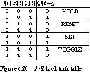
All input combinations lead to useful functions for the J-K
latch: hold, reset, set, and toggle. The characteristic equation is![]()
Notice how nicely the characteristic equation summarizes
the behavior of the J-K flip-flop. When J
= 1, K = 0, Q+ =
Q + ![]() , which is always 1
, which is always 1 (set).
Q+ is always 0 when J = 0, K =
1 (reset). Finally, when J =
1, K = 1, Q+ = ![]()
(toggle).
Problems with the Basic J-K
Flip-Flop If we actually built this circuit, we would \xde
nd an interesting problem as soon as the circuit is placed into the toggle
mode. The output toggles forever (or at least until one of
J or K returns to 0), as we show in Figure
6.21.
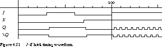
The problem is that the toggle signal remains asserted while the outputs
change, thus flipping the values of R and S presented
to the internal latch, causing it to toggle again. The process continues
until the toggle condition is removed.
Solution: Master/Slave Flip-Flop This
leads us to an alternative way to build a J-K memory element,
called a master/slave flip-flops. The basic idea is to build the memory
element in two stages. The first stage, the master, accepts new R-S
inputs and generates the outputs P and ![]() on the rising edge
of a clock signal. The second stage, the slave, accepts P and
on the rising edge
of a clock signal. The second stage, the slave, accepts P and ![]() as inputs on the falling edge of the clock and changes its outputs
after the falling edge. By the time the outputs propagate back to the \xde
rst stage, the clock signal has been removed, guaranteeing that the outputs
cannot toggle again
as inputs on the falling edge of the clock and changes its outputs
after the falling edge. By the time the outputs propagate back to the \xde
rst stage, the clock signal has been removed, guaranteeing that the outputs
cannot toggle again (at least not until the next rising clock
edge).
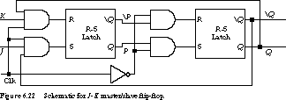
The schematic for this flip-flop is shown in Figure 6.22 and its associated
timing diagram is given in Figure 6.23.
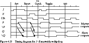
The timing diagram illustrates some important points
about J-K master/slave flip-flops. First, the P,
![]() outputs of the first stage track the Q,
outputs of the first stage track the Q,
![]() outputs of the second stage. The latter outputs change
a propagation delay after the falling edge of the clock signal. Second,
a general property of master/slave flip-flops is called ones catching.
If an input is high any time during the clock period, it will be interpreted
as a one for computing the output.
outputs of the second stage. The latter outputs change
a propagation delay after the falling edge of the clock signal. Second,
a general property of master/slave flip-flops is called ones catching.
If an input is high any time during the clock period, it will be interpreted
as a one for computing the output.
To see this behavior, let's trace the inputs and their
effect on the outputs. Initially the flip-flop has 0 as its output. J
goes high, and after the clock also goes high, P comes high. When
the clock goes low, P and ![]() are gated across to the
second stage, causing its output Q to go high. On the next rising
clock edge, J and K are both low, so the first stage holds
its state. Midway through the clock period, however, K comes high,
causing the first stage to reset. The 0 output is passed on to the second
stage, whose output goes low after the falling edge of the clock.
are gated across to the
second stage, causing its output Q to go high. On the next rising
clock edge, J and K are both low, so the first stage holds
its state. Midway through the clock period, however, K comes high,
causing the first stage to reset. The 0 output is passed on to the second
stage, whose output goes low after the falling edge of the clock.
The ones catching phenomenon is clearly shown in the next
input con-dition, where J changes from low to high to low while
the clock is asserted. Even though the input is back to zero by the time
the clock goes low, the output is still set. You must be careful when using
master/slave flip-flops with combinational logic that suffers from 0-hazards.
Any glitch at the inputs to the flip-flops could cause unintended state
changes.
If the latches are constructed from the NAND gates (that
is, ![]() -
-![]() latches
latches), there is
an analogous problem with zeros catching. If the clock is asserted
and the J or K input temporarily changes through zero,
the associated set or reset operation will take place.
The rest of the input configurations cause the outputs
to toggle from 1 to 0 to 1 to 0. Note that the outputs make only one state
change per clock period and that the output changes only after the falling
edge of the clock.
(positive
edge-triggered) or falling (negative
edge-triggered) clock edge. (this can be changed to
a positive edge-triggered device by using the clock's complement).
Unlike R-S and master/slave J-K devices,
a D flip-flop has only one data input. It stores the value presented
on this input when the clock signal performs the appropriate transition.
Its characteristic equation is simply Q+ =
D. Let's see how it works.
Operation of the D Flip-Flop The
operation of an edge-triggered device is considerably more complex than
that of the master/slave flip-flop. The circuit of Figure 6.24 contains
three communicating latches. The bottom latch samples the D input
while the top stage holds ![]() . The output from the bottom
latch drives the set input of the final stage latch, while the top latch
provides its the reset input.
. The output from the bottom
latch drives the set input of the final stage latch, while the top latch
provides its the reset input.
The figure shows the state of the circuit when the
clock is high. The clock forces the outputs of the top and bottom latches
to zero, thus keeping the final stage R-S latch in
its holding state. Any change in the D input will be sampled by
the top and bottom latches, but these changes are inhibited from affecting
the final stage latch.
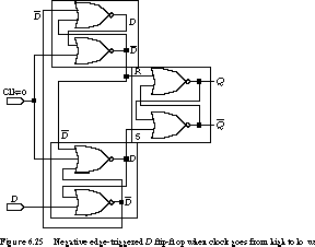
Figure 6.25 shows what happens when the clock initially changes from
high to low. The output NOR gates in the top and bottom latches now act
like inverters. The previously sampled value of D is presented
to the S input, while ![]() drives the R
input. If D
drives the R
input. If D = 1, the R-S latch outputs
a 1. Otherwise it outputs a 0.
What happens when the clock is low, but D changes?
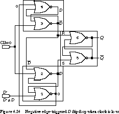
Figure 6.26 shows the state when the input changes to D', which
is different from the previously sampled value D. This new input
forces the output of the NOR gate to change from 1 to 0, since one input
must be a 1 and the other a 0. By driving this circuit node to 0, gates
2, 4, and 5 are guaranteed to hold their previous values. D' can
affect the circuit only when the outputs of gates 2 and 4 are forced to
0. This will happen only when the clock next goes high.
An examination of this circuit should make you appreciate
the need for setup and hold time specifications for flip-flops. If the
D input changes too close to the appropriate clock edge, its value
may not be held correctly by the top and bottom latches. Also, you can see
why the propagation delays may be rather substantial for these kinds of
devices.
We give a timing diagram for both positive and negative
edge-triggered devices in Figure 6.27.
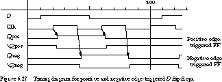
The outputs change after a small propagation delay from the rising or
falling edge. The last transition (time step 110)
shows how edge-triggered devices sample their inputs. In this case, the
input changes from a 0 to a 1 midway through the clock period. The change
goes undetected by the positive edge-triggered device-no ones catching here-but
is recognized by the negative edge-triggered flip-flop.
Toggle Flip-Flop There is still
one more kind of flip-flop: the toggle flip-flop, or T
flip-flop. The toggle flip-flop has a single input that causes the stored
state to be complemented when the input is asserted. Toggle flip-flops are
not usually found in standard parts catalogs because they are so easy to
construct from other flip-flop types. For example, a J-K
flip-flop with both inputs tied together will implement a T flip-flop.
If the input is 0, both J and K are 0 and the flip-flop holds its state; if the input is 1, both J and K are
1 and the flip-flops complements its state.
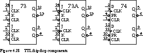
Figure 6.28 shows three of the most popular of these: the 7473 J-K
flip-flops and the 7474 D flip-flop. Each package contains dual
independent flip-flops. The '73 comes with independent active-low clear
signals (CLR/). When they are asserted, the flip-flop's
state is set to 0, independent of the current value of the inputs and the
clock. The '74 has both preset (PR/) and clear
(CLR/). In a similar way, when preset is asserted,
the flip-flop's state is set to 1.
The 7473 component comes in two versions: the standard
version contains master/slave flip-flops, and the "A" version
contains negative edge-triggered devices. The notation on the 7473A's clocks
shows you how to distinguish between edge-triggered and level-sensitive
operation. Edge triggering is denoted by a small triangle on the clock signal.
Negative edge triggering is denoted by the negation bubble on the clock
line. Be sure you are selecting the correct component for the job at hand.
The detailed timing behaviors of the 7473 and 7473A are not identical.
The 7474 is a positive edge-triggered D flip-flop.
The edge triggering of the clock is indicated by the triangle on the clock
signal. Without the bubble, the element is positive edge-triggered.
We usually form R-S latches from discrete
cross-coupled NOR gates using 7402 components. However, you can find four
![]() -
-![]() latches in a single package if you
use the 74279 component.
latches in a single package if you
use the 74279 component.
D flip-flops are almost universally available
in positive edge-triggered configurations. What if you need a negative edge-triggered
device? One solution is to invert the clock signal on the way into a D
flip-flop like the 7474. An alternative is to use a negative edge-triggered
J-![]() flip-flop, such as the 74276. By simply wiring the J
and
flip-flop, such as the 74276. By simply wiring the J
and ![]() inputs together, you can construct a D flip-flop.
inputs together, you can construct a D flip-flop.
[Top] [Next]
[Prev]