(1) the correct
input values, with respect to time, are provided to the flip-flops that
are changing their states, and (2) no flip-flop
should change its state more than once during each clocking event.
What rules should we follow for composing synchronous systems to guarantee these two properties?
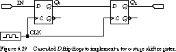
Figure 6.29 illustrates the problem. Here, we cascade two D flip-flops so that the output from the first stage feeds the input to the second stage. Both flip-flops are controlled by the same clock signal. The purpose of this circuit is to transfer the current state of the first stage to the second stage while the first stage receives a new value. In other words, the second stage contains the value stored in the first stage during the previous clock period. This is an example of a shift register, a multibit memory with a capability of exchanging a single memory element's contents with its neighbors. We will see more of shift registers in Chapter 7.
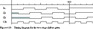
The proper logic operation of the circuit is shown in Figure 6.30, assuming that the flip-flops are positive edge-triggered and that the input stream is 0101011. Initially, both flip-flops contain unknown values. On the first rising edge of the clock, the input is 0 and appears at output Q0 a short propagation delay later. The state of the second flip-flop is still unknown.
On the second rising clock edge, the input is 1, and
Q0 takes on this value some propagation delay after the clock edge.
However, at the clock edge, the second stage sees the old value of Q0
as its input. Thus, Q1 becomes zero shortly after the rising edge.
The pattern continues through the diagram. Q1 always displays the
value that Q0 had just before the rising clock edge.
We would not observe proper transfer of data between
the stages if the first was positive edge-triggered while the second
stage was negative triggered. After the first clock cycle, we would have
0 in both flip-flops. After the second cycle, both flip-flops
would hold a 1, and so on. It is not good design practice to mix flip-flops that are sensitive to different timing events within the same circuit!
Proper Cascading of Flip-Flops In
general, we assume that the propagation of the clock signal is infinitely
fast and that all flip-flops have identical timing. In real circuits,
this isn't true. Some components may be faster than others, and the wire
delay for distributing a signal to all points where it is needed may vary
substantially. Let's suppose that the first-stage flip-flop has
a very fast propagation delay, so fast in fact that the new value of Q0
appears at the input to the second stage before it had a chance to observe
the previous value of Q0. We would not be properly passing the
value from stage to stage in this case.
The same problem arises if the connection between the
clocks of the two flip-flops is a long meandering wire, while the
output of stage one and the input to stage two are connected by a very short
wire. It is only after the first stage has changed its value that the
second stage receives the clock transition. Thus, the stages will have incorrectly
latched the same value. Such a circuit violates our basic assumption that
all flip-flop inputs are examined simultaneously.
Fortunately, the designers of TTL components have built
them so they can be cascaded without timing problems (this
is true as long as the same families of TTL components and the same kinds
of clocking events are used). It is important to remember that
the inputs must be held stable for a setup time before and a hold time after
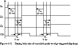
the clock edge. For the 74LS74 positive edge-triggered flip-flop,
these are 20 ns and 5 ns, respectively. Fortuitously, the propagation delay
far exceeds the hold time. In the 74LS74 case, the typical delay for a low-to-high
transition is 13 ns. Unless the clock signal to the second stage is delayed
by more than 7 ns, the first stage cannot change its value and propagate
it to the second stage before the hold time has expired. By then, the second
stage has successfully latched the original Q0 value. This timing
behavior is shown in Figure 6.31.
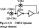
These latches are called dynamic storage elements because the
clock must continue to run for the element to hold its current value. Static
storage elements, such as the TTL flip-flops, hold their value
independent of the oscillations of the clock and continue to do so as long
as power is applied to the circuit.
Compare Figure 6.32, a dynamic D-type storage
element, and Figure 6.24, a static edge-triggered D flip-flop. The former is much more transistor efficient than the latter. The
two alternative approaches lead to quite different clocking strategies.
Edge-triggered devices are easy to use and require only a simple oscillating
clock signal. Level-sensitive latches, on the other hand, place special
restrictions on the clock signal, as we will see next.
Clocked Sequential Systems with Latched State Flip-flops are the most primitive form of circuits with feedback. There are several ways to generalize these to more complex sequential networks. Throughout this section, we will focus on more general clocked sequential systems, as shown in Figure 6.33.
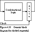
Clocked sequential systems consist of a block of memory
elements (state) driven by combinational
logic whose inputs include the current contents of the memory elements.
The feedback path from the state to the combinational logic inputs could
cause multiple state changes unless we design the clocking method carefully.
Proper operation of the circuit requires that the state changes only once
per clock cycle.
To see how a problem can happen, let's consider an example.
The arrival of the clocking event causes the new state to replace the current
state. If there is some way that this new state can race through the combinational
logic and cause a second new state to be computed, all within the same clock
period, we have violated one of our requirements for proper operation. As
in the R-S latch, the new state depends on the timing
of the circuit, as well as the inputs and the current state. Sometimes the
state may change once per clock period and sometimes more than once, depending
on the delay paths through the logic. The new state cannot be determined
unambiguously.
This problem will not occur in edge-triggered systems.
The time that the clock edge is in transition is small compared to the clock
period and any associated logic delays. So fast signals are not a problem.
However, if the state storage elements are implemented
with level-sensitive latches, we must use a clocking methodology based on
narrow clock widths. The clock high time is small compared to the clock
period.
When implemented with a narrow-width clock, a clocked
sequential system behaves as follows. Whenever the clock goes high, the
current state is replaced by a new state as the state memory elements latch
a new value. If the clock remains high long enough for the new state to
race back to the input of the combinational logic and propagate through
it, we could observe a double state change. To ensure that this never takes
place, we must use a clock whose high time is less than the fastest
possible path through the combinational logic. This is measured from
the rising edge of the clock and should include the delay through the state
latch.
To guarantee that the correct next state has been computed, we also make sure that the period of the clock is longer than the worst-case propagation delay through the combinational logic. Because the next state signal actually has until the end of the high time of the clock to be computed, this constraint can be measured up to the falling edge of the clock, as long as the latch setup time is included. The constraints are shown in Figure 6.34.
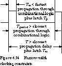
Tw is the high time of the clock, Tperiod is the clock period, and T is the time from when the clock first goes high until it goes low in the next period.
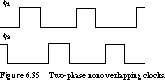
An Alternative to Narrow-Width Clocking: Multiphase Clocking Narrow-width clocking forces the designer to think about fast as well as slow paths through the logic. Finding these critical delays is even more of a problem because they vary with temperature and other environmental factors. An alternative is to use multiple-phase nonoverlapping clocks, the simplest case being a two-phase scheme. An example of a two-phase clock waveform is shown in Figure 6.35.
If we apply the two-phase scheme to the general clocked sequential system block diagram of Figure 6.33, we get the system shown in Figure 6.36.
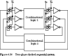
Each feedback path passes through a pair of inverters. And each inverter
pair implements a dynamic storage element, as in Figure 6.32. (The
second block of combinational logic is optional.)
By breaking every feedback path with both phases of the
clock, we eliminate the possibility of signal races. Since both clocks are
never high at the same time, a feedback signal cannot possibly pass through
the combinational logic block more than once in any j1/j2
cycle. We need only ensure that the periods of j1 and j2
are greater than the worst-case delay found in combinational logic blocks
2 and 1 (plus the appropriate latch setup times).
This system is an improvement over narrow-width clocking.
We need only worry about the slow signals. Unfortunately, the multiphase
scheme requires more clock signals to be distributed and routed throughout
the system.
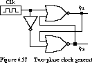
Generating nonoverlapping clocks is not particularly difficult, as the circuit of Figure 6.37 and the timing diagram of Figure 6.38 demonstrate.
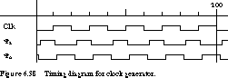
The circuit works as follows. The rising edge of the external clock forces
j1 to go low. The feedback from the j1 output
to the lower NOR gate allows that phase to go high. When the external clock
goes low, the process is repeated for the high-to-low transition of j2,
feeding back to allow j1 to come high. In the timing diagram,
the nonoverlap time is only a single gate delay. This may not be suf\xde
cient to avoid offsets in the timing of the clock waveforms due to different
wire distribution delays for the two phases. This problem is called clock
skew, and it is discussed in the next subsection. To increase the nonoverlap
time, we simply place additional delay in the feedback path. An even-numbered
chain of inverters is a good way to implement this delay.
Summary Whereas latches may be transistor
efficient in VLSI implementations, there is usually no area advantage
in packaged logic like TTL. You get just about as many edge-triggered flip-flops per package as you get latches. Therefore, most modern TTL designs
use edge-triggered flip-flops, and a single-phase clock is all you
need. To avoid problems in transferring signals from one type of flip-flop to another, we strongly advise that the system be constructed from all
positive edge-triggered or all negative edge-triggered devices.
Suppose that the original state of both flip-flops is 1 and that the input to the flip-flop is 0. If the circuit behaves correctly, the state of the first flip-flop should change from 1 to 0 while the second flip-flop stays at 1 (its current value of 1 is replaced by the old value of the first flip-flop, which is also 1).
The timing diagram of Figure 6.39 shows what really happens.
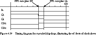
The first flip-flop is reset to 0, but so is the second flip-flop! This
occurs because the second stage sees the new state of the first stage (0),
rather than its current state (1), by the time
CLOCK2 arrives.
Avoiding Clock Skew One way
to avoid clock skew is to route the clock signal in a direction opposite
to the flow of data. For example, we could arrange the clock signal so that
it arrives at the second flip-flops before the first. The second flip-flop
would then change its state based on the current value of the first stage.
There is no problem if the first stage changes its state well after the
second stage.
Unfortunately, this may not be too helpful, since most
communications move in both directions. This means that skew will be a problem
in one of them.
Because the typical propagation delay for the LS family
of TTL components is 13 ns, the skew needs to be rather substantial for
the second stage to read the wrong value. (Of course, skew
becomes more of a problem with faster systems or those that span a larger
circuit area.) The best plan is to route the clock signals
so that components that communicate with each other are connected via short
clock lines.
[Top] [Next]
[Prev]